Google's 'Frozen v2' Chip: Why Hardwiring Gemini Could Cut AI Power Use 6–10x

Google's 'Frozen v2' Chip: Why Hardwiring Gemini Could Cut AI Power Use 6–10x
The Information reported on July 20, 2026 that Google is developing a server chip codenamed "Frozen v2" that could be six to ten times more power-efficient than its latest TPUs — by burning parts of Gemini's model architecture directly into the silicon. Alphabet stock rose more than 3% on the news. This post explains what "hardwiring a model" actually means, why it trades flexibility for efficiency, how it fits Google's TPU roadmap, and whether it's a real threat to Nvidia or a science experiment. Deployment isn't expected until 2028, and Google itself reportedly treats it as a trial run.
Most AI chips, including Google's own TPUs, are built to run any model you load onto them. Frozen v2 is the opposite idea: a chip designed to run essentially one model — Gemini — and to do it so efficiently that Google is willing to give up general-purpose flexibility to get there. That's a genuinely different bet from the AI-chip arms race everyone's been watching. Below is what's confirmed, what's still just a report, the trade-off that defines the whole thing, and the honest read on what it means for Nvidia.
Table of Contents
- What 'Frozen v2' Actually Is
- The Trade: Efficiency vs Flexibility
- Where It Fits Google's Chip Roadmap
- Does This Actually Threaten Nvidia?
What 'Frozen v2' Actually Is
The report comes from The Information and was picked up by Reuters, CNBC, and TechCrunch on July 20, 2026. The core claim: Google is developing a server chip, codenamed Frozen v2, that could be six to ten times more power-efficient than Google's latest TPUs for running Gemini.
The mechanism is what makes it unusual. Instead of a flexible processor that loads a model's weights from memory and computes on them, Frozen v2 reportedly hardwires parts of Gemini's architecture directly into the silicon. By fixing pieces of the model into the chip's physical circuits, it slashes two of the biggest energy costs in AI inference: raw computation and the constant shuttling of data back and forth to memory.
Here's the honest fact-versus-report line. The existence of the project, the 6–10x efficiency framing, the 2028 target, and the "trial run" characterization all come from a single report (The Information), not a Google product announcement. Google has not officially confirmed the chip. What is independently confirmed is the market reaction: Alphabet (GOOGL) rose more than 3% on the day, with the move widely tied to the report. Treat the technical specifics as credible reporting, not settled fact.
Three caveats sit right in the reporting itself, and they matter:
- Timeline: deployment is reportedly targeted for 2028, not this year — this is a roadmap item, not a shipping product.
- Scale: Google reportedly does not plan to produce Frozen v2 at the same volume as its TPUs; it's partly a trial run.
- Fragility: the chip would only work with future Gemini models if Google keeps the same underlying architecture. Change the architecture meaningfully and the hardwired chip loses its advantage.
## The Trade: Efficiency vs Flexibility
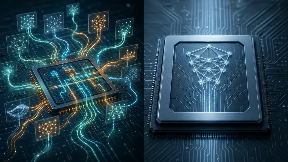
Every specialized chip is a bet that a workload has stopped changing. The more you fix into silicon, the faster and more efficient you get — and the more badly you lose if the workload shifts. Frozen v2 pushes that trade further than almost anything on the market, because it specializes not just to a type of model (transformers) but to essentially one specific model family (Gemini).
Here's the trade laid out directly:
| Dimension | General-purpose TPU (Google's current chips) | Model-hardwired chip (Frozen v2) |
|---|---|---|
| What it runs | Any model — training and inference | Primarily one model family (Gemini) |
| Power efficiency on Gemini | Baseline | Reportedly 6–10x better |
| Adapts to new model architectures | Yes, load new weights | No — advantage tied to fixed architecture |
| Risk if the model changes | Low | High — efficiency edge can evaporate |
| Production scale (reported) | Full scale | Trial run, limited volume |
The logic is the same one behind Bitcoin mining ASICs and behind AI-chip startups like Etched, which hardwires transformers into fixed silicon. (Related: Etched's Jump From $5B to $20B: What a Transformer-Only AI Chip Means for Nvidia's Grip.) Frozen v2 is a step even more extreme: Etched freezes an architecture, Google is reportedly freezing pieces of an actual model. That's why the "trial run" framing is rational — you don't commit your whole fleet to a chip whose usefulness depends on your flagship model's design staying frozen for years.
The payoff, if it works, is enormous where it counts. Inference — serving a trained model to users, over and over — is the cost that never stops growing; it scales with every single query. A 6–10x cut in the power needed to run Gemini at Google's scale would translate directly into lower data-center electricity bills, less pressure on grid capacity, and a structural cost advantage over rivals renting Nvidia GPUs by the hour.
Where It Fits Google's Chip Roadmap
Frozen v2 isn't Google's main chip strategy — it's an experimental branch off a very mature tree. Google already runs one of the industry's most advanced custom-silicon programs:
- Ironwood, Google's seventh-generation TPU, reached general availability as the first TPU purpose-built for what Google calls the "agentic era" of large-scale inference.
- Google has previewed an eighth generation: two chips, TPU 8t for training and TPU 8i for inference, both targeting TSMC's 2nm process and expected to reach general availability later in 2026. Broadcom is reportedly designing the training chip and MediaTek the inference chip.
Against that backdrop, Frozen v2 reads as a research bet layered on top of a shipping roadmap, not a replacement for it. Reporting explicitly frames it as complementing TPUs, not replacing them. The strategic thread running through all of it is the same: Google wants to reduce its AI infrastructure costs and lessen its reliance on Nvidia's GPUs, and owning the whole stack — from the model down to the transistor — is how it plans to do that.

## Does This Actually Threaten Nvidia?
Not directly, and not soon — but it's another crack in the same wall. Nvidia's dominance is anchored in training, where its market share still exceeds 90% of the merchant market and CUDA's software ecosystem is close to non-negotiable. Frozen v2 doesn't touch training at all. It's aimed squarely at inference, the slice where Nvidia's grip is already looser — estimated in the 60–75% range — as TPUs, AWS Trainium, and AMD's accelerators have found real commercial traction on cost-sensitive workloads.
Zoom out and the trend is unmistakable even without Frozen v2. Nvidia's overall AI-accelerator share peaked near 87% in 2024 and is projected around 75% for 2026 (IDC pegs its AI data-center chip share near 81%). Custom ASICs are on track to make up roughly 27.8% of accelerator server shipments in 2026, the highest share since 2023, and Broadcom's AI backlog alone sits near $73 billion with a target of $100 billion in annual AI revenue by 2027. Frozen v2 is one more data point in a broader migration of hyperscalers toward their own silicon for inference.
So the realistic read: Frozen v2 won't dethrone Nvidia, and it isn't even trying to — it's a Google-internal efficiency play that only helps Google run Gemini cheaper. But every hyperscaler that gets better at serving its own models on its own chips shrinks the addressable market Nvidia has been pricing as if it owns forever. The threat to Nvidia isn't one heroic chip; it's the accumulation of many of them.
Frequently Asked Questions
Is Frozen v2 available now? No. It's a reported project with deployment targeted for 2028, and Google reportedly treats it as a trial run rather than a mass-production chip. Google has not officially confirmed it.
How is it different from a normal TPU? A TPU is general-purpose — it can run any model you load. Frozen v2 reportedly hardwires parts of Gemini's architecture into the silicon itself, making it far more efficient at running Gemini but far less flexible for anything else.
Does 6–10x more efficient mean it's 6–10x faster? Not necessarily. The reported figure is about power efficiency — energy used per unit of work — not raw speed. For a company running AI at Google's scale, energy per query is often the number that matters most for cost.
Why would Google build a chip that only runs one model? Because inference cost scales with every user query, and Gemini is Google's flagship. If Gemini's architecture stays stable, a chip tuned exactly to it can run cheaper than a general chip — a large structural advantage at Google's volume.
Does this hurt Nvidia? Only indirectly. It targets inference, where Nvidia's share is already weaker (60–75%), not training, where Nvidia still holds 90%+. It's one more hyperscaler moving inference onto in-house silicon.
Key Takeaways
- Google is reportedly developing Frozen v2, a chip that hardwires parts of Gemini into silicon for a claimed 6–10x power-efficiency gain over its latest TPUs.
- The mechanism cuts computation and memory data movement — the two biggest energy costs in AI inference.
- It's a trade: extreme efficiency in exchange for extreme specialization; the edge depends on Gemini's architecture staying stable, and deployment isn't targeted until 2028.
- It complements Google's TPU roadmap (Ironwood, plus 2nm TPU 8t/8i), rather than replacing it.
- It doesn't threaten Nvidia's training dominance (90%+ share) but adds to the slow erosion of its inference share (60–75%) as hyperscalers build their own chips. Alphabet stock rose 3%+ on the report.
How this was written: Research and a first draft came together with AI's help; verification and the final pass were entirely human.
References
- The Information / Reuters, "Google plans new chip to run Gemini models more efficiently" (July 20, 2026): https://www.reuters.com/technology/
- CNBC, "Alphabet stock pops on report it's developing a more efficient AI chip" (July 20, 2026): https://www.cnbc.com/2026/07/20/alphabet-googl-stock-ai-chip-report.html
- TechCrunch, "Google is working on a new AI chip designed to make Gemini more efficient" (July 20, 2026): https://techcrunch.com/
- Stocktwits, "Alphabet Stock Gains On Report Of Google's New 'Frozen' Chip": https://stocktwits.com/news-articles/markets/equity/alphabet-googl-stock-google-frozen-v2-gemini-ai-chip/cZZiBQ2R7uU
- Tom's Hardware, "The custom AI ASIC state of play (May 2026)": https://www.tomshardware.com/tech-industry/semiconductors/custom-ai-asics-examined-from-broadcom-to-mtia
- gomarkets, "NVIDIA vs Google TPU: The AI chip war investors are watching": https://www.gomarkets.com/en/articles/google-tpu-chips-and-nvidia-the-ai-chip-war


Comments ()